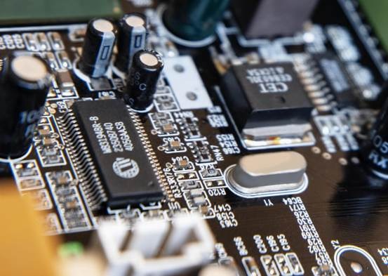
As electronics become smaller and faster, designers face a simple problem — how to fit more performance into less space. That’s where high density interconnect pcb technology comes in. HDI boards enable routing fine-pitch components, managing high-speed signals, and meeting mechanical constraints for small form factors such as smartphones, wearables, and automotive modules.
In this article, we’ll break down what HDI really means, how stackups are built, the key design rules for manufacturability, and why choosing the right fabrication partner can make or break your project.
What Is HDI and Why Does It Matter?
HDI stands for High Density Interconnect. These PCBs use thinner traces, smaller vias, and more layers to achieve higher wiring density than standard multilayer boards. HDI combines microvias, blind and buried vias, and sequential lamination to increase circuit density while maintaining excellent signal integrity.
Compared to traditional multilayer PCBs, HDI offers:
- Higher component density – perfect for fine-pitch BGAs and chip-scale packages.
- Shorter signal paths – improving speed and reducing noise or crosstalk.
- Lighter, smaller assemblies – ideal for portable and automotive electronics.
HDI is the backbone of today’s advanced electronics, balancing performance, reliability, and compactness.
Typical HDI Structures
The most common HDI stackups are 1+N+1 and 2+N+2, where “N” represents the number of core layers. A 1+N+1 design uses one build-up layer on each side of the core, which keeps costs low while still enabling microvia routing for fine-pitch components.
More complex designs use 2+N+2 or even stacked microvias to achieve extreme density. These stackups enable escape routing from high-I/O BGAs and complex IC packages.
HDI fabrication typically involves sequential lamination, laser-drilled microvias, and copper filling or resin plugging to ensure flat, reliable via pads.
At FastTurn PCB, engineers can build 1+N+1 and 2+N+2 configurations with up to 18 layers, supporting a variety of blind, buried, and stacked microvia designs.
Key Design Rules for Manufacturability
Design for Manufacturability (DFM) is essential in HDI. Following these baseline rules can help avoid production delays and improve yield:
- Trace width and spacing: Aim for 2.5/2.5 mil (0.063/0.063 mm) for stable, high-yield production.
- Microvia size: Laser-drilled vias as small as 0.10 mm (4 mil) in diameter with 0.20 mm pads are practical and cost-effective.
- Aspect ratio: Keep microvia depth-to-diameter ≤ 1:1 to ensure consistent plating.
- Via-in-pad: Use copper-filled or resin-plugged vias with a flatness tolerance within ±10 μm for better solder joint reliability.
- Impedance control: Define 50-ohm single-ended or 100-ohm differential pairs early in the design and verify stackup with your fabricator before layout is finalized.
Signal Integrity, Power, and Thermal Management
As rise times get faster, HDI design must protect signal integrity (SI) while maintaining good power distribution (PDN) and heat dissipation.
- Signal Integrity (SI): Keep differential pairs length-matched and reference planes solid. Avoid unnecessary via transitions and maintain controlled impedance along high-speed paths.
- Power Distribution (PDN): Use wide copper pours, solid planes, and local decoupling capacitors to stabilize supply voltages.
- Thermal Management: Select the proper copper thickness (1–6 oz) and use thermal vias under power components to evenly distribute heat.
By integrating these practices, HDI boards deliver stable electrical and thermal performance even in dense, high-power systems.
Materials and Processes
HDI performance depends heavily on the materials used. High-Tg FR-4 and low-loss laminates support both mechanical reliability and signal integrity at high frequencies.
FastTurn PCB offers RoHS- and REACH-compliant materials with optional halogen-free (HF) systems and UL94V-0 flame rating. Precise sequential lamination control (±2 °C temperature and ±0.1 bar pressure) ensures layer-to-layer consistency, while 0.15 mm (6 mil) finished through-holes expand design flexibility.
From DFM review to impedance simulation, sample validation, and volume production, the company maintains a closed-loop manufacturing process that minimizes risk and improves repeatability.
Capability Benchmarks
Here’s a quick reference for manufacturable HDI parameters based on FastTurn’s standard process:
| Minimum Line/Space | 2.5 / 2.5 mil |
| Microvia Hole | 0.10 mm (Pad 0.20 mm) |
| Aspect Ratio | ≤ 1:1 |
| Max. HDI Stack-Up | Up to 18 layers |
| Through-Hole | Finished Ø 0.15 mm (6 mil) |
| Impedance Tolerance | ± 5 Ω / ± 10 % |
| Copper Thickness | 1 – 6 oz |
| Board Thickness | 0.4 – 3.2 mm |
These benchmarks help designers check whether their layout fits realistic fabrication windows before release.
Applications That Benefit from HDI
HDI technology is widely used wherever compact size and high performance meet. Typical industries include:
- Consumer electronics – smartphones, tablets, wearables.
- Automotive – ADAS cameras, radar modules, and infotainment.
- Medical – imaging, portable diagnostic devices.
- Industrial and communications – routers, sensors, test systems.
For high-speed signals and tight component spacing, HDI delivers performance and miniaturization without compromising reliability.
Frequently Asked Questions
1. What’s the main difference between HDI and traditional multilayer PCBs?
HDI uses microvias, blind/buried vias, and finer lines to achieve much higher routing density and better electrical performance.
2. How do I choose between 1+N+1 and 2+N+2?
1+N+1 is suitable for moderate-density designs; 2+N+2 or stacked microvias are used for fine-pitch BGAs and higher-I/O chips.
3. Are via-in-pad designs required for HDI?
Not always, but they help shorten connections and improve thermal paths. Copper-filled via-in-pad gives the best reliability.
Conclusion
HDI technology is now standard in industries demanding compact, high-speed, and reliable PCBs. Understanding stackups, design rules, and manufacturable limits helps engineers balance performance and cost from the start.
When you’re ready to move from concept to production, partner with FastTurn PCB. Their engineering team can review your HDI design, suggest stackup adjustments, and deliver prototypes or production boards that meet your reliability and timeline goals.